
Embedded Systems and PCB Design
- Başak Karadağ
- Mar 19, 2025
- 2 min read
The Embedded Systems Group of our team works on the design, assembly, and software integration of low-voltage circuit boards in our vehicle. Printed Circuit Boards (PCBs), one of the fundamental building blocks of embedded systems, are not only structures that carry hardware components but also serve as the physical platform where embedded software is executed.

What is a PCB (Printed Circuit Board) and Why is it Important?
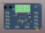
A PCB (Printed Circuit Board) is a board consisting of conductive copper traces and insulating layers that connect the components of an electronic circuit. This board ensures that the circuit components are interconnected as designed, allowing for the creation of more compact, reliable, and efficient electronic circuits compared to traditional wired connections. In the Solar Car, PCBs house many critical components, including microcontrollers, communication modules, power management circuits, and sensors. Therefore, both electrical and mechanical design requirements must be considered during the PCB design process.

How Does the PCB Design Process Progress?
Needs Analysis and Planning
The PCB design process begins with defining the electrical system requirements of the vehicle, ensuring compliance with competition regulations, managing power consumption, and determining the communication protocols to be used in the vehicle. A design concept is developed to meet these parameters. During this stage, both electrical and electronic principles, as well as potential mechanical constraints, are considered. Based on these criteria, suitable components are selected for the boards. We also test circuits using circuit simulation applications during the design process.
Schematic Preparation and PCB Design
A circuit schematic is created for the PCB to be designed in accordance with the defined design constraints and requirements. At this stage, it is crucial to ensure that the schematic is correctly structured and that the connections are made following the design recommendations specified in the datasheets of the integrated components used on the PCB. Once the schematic is completed, the PCB layout process begins. This phase is critically important, as it involves the proper placement of circuit components, the establishment of reliable signal paths, and the management of high-frequency components to prevent unwanted factors such as noise. Additionally, calculations for traces carrying high voltage and current must be conducted carefully. Furthermore, challenging conditions such as vibrations and high temperatures that the Solar Car may encounter during the race directly impact the design process.

PCB Manufacturing, Software Integration, and Testing
After the PCB design is completed, the boards are sent for manufacturing. Once produced, they are soldered in the workshop, and the microcontrollers on the board are programmed with software designed to process sensor data, facilitate communication via predefined protocols (CAN, UART, SPI, I2C), and ensure the board performs its intended functions. The testing phase then begins, conducted both outside the vehicle and within the vehicle itself, considering various parameters and race conditions. This step is crucial to verify that the system operates as designed in theory and to ensure the board functions reliably in real-world conditions.
Continuous Improvement and Team Collaboration
By maintaining constant interaction with other groups, we aim to improve our PCB designs based on feedback and enhance the overall performance of the system.
This process, requiring a professional approach and meticulous planning at every stage, not only makes us competitive in races but also represents a significant step toward contributing to the future of energy solutions.